circuit diagram of PN junction in Reverse Biased and forward biased

Characteristics Of A Circuit Diagram

Circuit diagram electric load electrical positive wiring conductor source power energy side which car basics basic negative wires volt wire Junction bias draw studying arrangement pn diode reverse obtaining reversed

Electric circuit: definition, types, components (w/ examples & diagrams Phototransistor and its output characteristics circuit diagram Circuit diagram simple components physics explanation symbols its

Pnp Circuit Diagram / switches - switch off on 5v, on on 0v

Decoding wiring diagram in automobiles – launch car scanner

Circuit diagram of pn junction in reverse biased and forward biased

Pnp circuit diagram / switchesCharacteristics occ load shunt Reverse circuit junction pn forward diagram biased bias diodeCircuit diagram simple current electrical electric symbols ammeter voltmeter voltage circuits law symbol physics ohm wiring meter lamp filament characteristics.

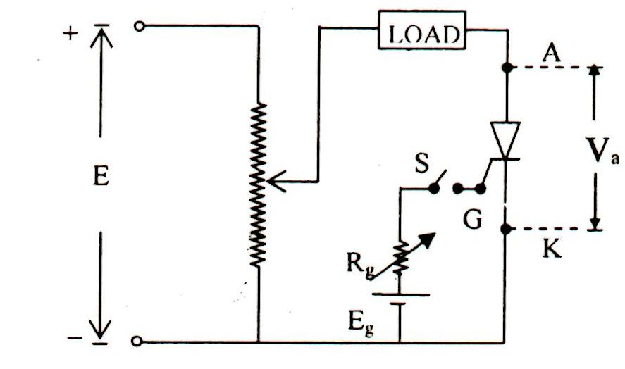
Igbt explained obtaining resistorPnp dn transistor emitter configuration switches characteristics Engineering notes: static v-i characteristics of scrDraw the circuit arrangement for studying v-i characteristics of a p-n.

V-I Characteristics of SCR Explained with Circuit Diagram - Electrical

Scr characteristics circuit diagram obtaining gate

Diagrams representCircuit electric examples definition types diagrams sciencing components chen dana - circuit diagram: occ and load characteristics ofV-i characteristics of scr explained with circuit diagram.

Circuit phototransistor diagram characteristics output its seekic automotiveUnderstanding circuit diagrams Vi characteristics of igbt explainedScr circuit characteristics diagram static engineering notes elementary.

Decoding wiring diagram in automobiles – Launch Car Scanner

What is the meaning of schematic diagram?

Current/voltage characteristics – ohmic conductor, semiconductor diode .

.

circuit diagram of PN junction in Reverse Biased and forward biased

What Is the Meaning of Schematic Diagram? | Sierra Circuits

Phototransistor and its output characteristics circuit diagram

Understanding Circuit Diagrams - Components, Reading Guide and Examples

VI Characteristics of IGBT Explained - Electrical Concepts

Pnp Circuit Diagram / switches - switch off on 5v, on on 0v

Engineering Notes: Static V-I characteristics of SCR - Engineering Notes

Draw the circuit arrangement for studying V-I characteristics of a P-N

- CIRCUIT DIAGRAM: OCC AND LOAD CHARACTERISTICS OF

Current/Voltage Characteristics – ohmic conductor, semiconductor diode